- 您现在的位置:买卖IC网 > Sheet目录502 > QSE257 (Fairchild Semiconductor)IC PHOTOSENSOR SIDELOOKER
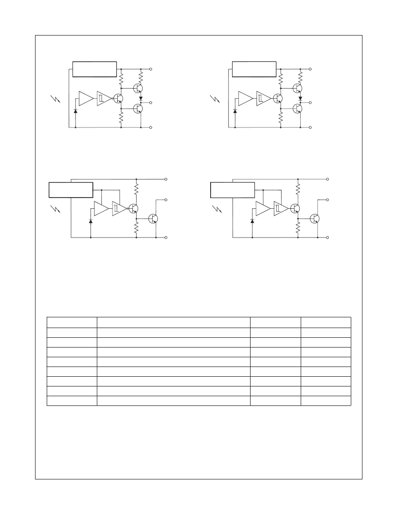
Block Diagrams
VOLTAGE
REGULATOR
LA
V CC
V OUT
VOLTAGE
REGULATOR
LA
V CC
V OUT
QSE256
Totem-Pole Output Buffer
VOLTAGE
REGULATOR
LA
QSE258
Open-Collector Output Buffer
GND
V CC
V OUT
GND
GND
QSE257
Totem-Pole Output Inverter
VOLTAGE
REGULATOR
LA
QSE259
Open-Collector Output Inverter
V CC
V OUT
GND
Absolute Maximum Ratings (T A = 25°C unless otherwise speci?ed)
Stresses exceeding the absolute maximum ratings may damage the device. The device may not function or be
operable above the recommended operating conditions and stressing the parts to these levels is not recommended.
In addition, extended exposure to stresses above the recommended operating conditions may affect device reliability.
The absolute maximum ratings are stress ratings only.
Symbol
T OPR
T STG
Parameter
Operating Temperature
Storage Temperature
Rating
-40 to +85
-40 to +100
Unit
°C
°C
T SOL-I
Soldering Temperature
(Iron) (2,3,4)
240 for 5 sec
°C
T SOL-F
I O
V CC
V O
P D
Soldering Temperature (Flow) (2,3)
Output Current
Supply Voltage
Output Voltage
Power Dissipation (1)
260 for 10 sec
50
4.0 to 16
35
100
°C
mA
V
V
mW
Notes:
1. Derate power dissipation linearly 2.50mW/°C above 25°C.
2. RMA flux is recommended.
3. Methanol or isopropyl alcohols are recommended as cleaning agents.
4. Soldering iron tip 1/16" (1.6mm) minimum from housing.
?2004 Fairchild Semiconductor Corporation
QSE256, QSE257, QSE258, QSE259 Rev. 1.0.1
2
www.fairchildsemi.com
发布紧急采购,3分钟左右您将得到回复。
相关PDF资料
QSE258
IC PHOTOSENSOR SIDELOOKER
QSE259
IC PHOTOSENSOR SIDELOOKER
QSE773E3R0
PHOTODIODE GAAS 940NM SIDELOOKER
QSE973E3R0
PHOTODIODE SIDELOOKER PIN TO-92
QTLP610CIRTR
EMITTER RA 940NM SMD
QTLP610CPDTR
EMITTER RA 940NM SMD
R5013ANXFU6
MOSFET N-CH 500V 13A TO-220FM
R5016ANX
MOSFET N-CH 500V 16A TO-220FM
相关代理商/技术参数
QSE258
功能描述:光IC传感器 OPTOLOGIC SIDELOOKER BUFFER OPEN COLLECT
RoHS:否 制造商:Honeywell 产品:Photo IC 通道数量:1 输出类型:10 KOhms Pull-up, Inverter 工作电源电压:4.5 V to 16 V 电源电流:12 mA to 15 mA 高电平输出电流: 上升时间:60 ns 下降时间:15 ns 传播延迟时间:5 us 最大工作温度:+ 100 C 最小工作温度:- 40 C 标准包装数量: 封装:
QSE259
功能描述:光IC传感器 2.4MHZ 4.5A TINYBUCK SYNCHRONOUS BUCK
RoHS:否 制造商:Honeywell 产品:Photo IC 通道数量:1 输出类型:10 KOhms Pull-up, Inverter 工作电源电压:4.5 V to 16 V 电源电流:12 mA to 15 mA 高电平输出电流: 上升时间:60 ns 下降时间:15 ns 传播延迟时间:5 us 最大工作温度:+ 100 C 最小工作温度:- 40 C 标准包装数量: 封装:
QSE-40-01-C-D-A-K
制造商:SAMTEC 制造商全称:Samtec, Inc 功能描述:0,80mm HI-SPEED SOCKET
QSE-40-01-C-D-A-RT1
制造商:SAMTEC 制造商全称:Samtec, Inc 功能描述:0,80mm HI-SPEED SOCKET
QSE-40-01-C-D-A-TR
制造商:SAMTEC 制造商全称:Samtec, Inc 功能描述:0,80mm HI-SPEED SOCKET
QSE-40-01-F-D-A
制造商:Samtec Inc 功能描述:CONN SCKT STRP SKT 80 POS 0.8MM SLDR ST SMD - Bulk
QSE-40-01-F-D-A-K
制造商:SAMTEC 制造商全称:Samtec, Inc 功能描述:0,80mm HI-SPEED SOCKET
QSE-40-01-F-D-A-RT1
制造商:SAMTEC 制造商全称:Samtec, Inc 功能描述:0,80mm HI-SPEED SOCKET
